|
|
|
68HC11 Assembly Language ProgrammingThis chapter introduces the inner workings of the 68HC11 microprocessor, and provides details on writing assembly language programs for the 68HC11. Since most, if not all, programming for ELEC 201 will be in IC most ELEC 201 readers can just skim this material for background information. This chapter is adapted from the `` 68HC11 PROGRAMMING GUIDE'', written by Fred Martin of M.I.T. Bits and BytesMost humans, having ten fingers, think in decimal numbers. In computers, information is represented with voltages, and it is most convenient for the voltage levels to represent only two states: a binary one or binary zero. Thus computers process binary digits, or bits. For convenience, microprocessors group bits together into words. The first microprocessor, the Intel 4004, operated on a word composed of four bits. Today, most microprocessors use eight bit words, called bytes. In an eight bit numeral, 256 different states can be represented (). Programmers use these 256 states to represent different things. Some common usages of a byte of data are:
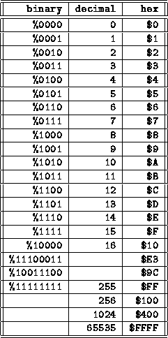
When programmers need to represent larger numerals, they group bytes together. A common grouping is two bytes, often called a (16-bit) word. A word can have 65536 states, since . Decimal numbers are painful to use when talking about binary information. To make life easier, programmers started to use the base 16 hexadecimal (or hex for short) numbering system when talking about bits, bytes, and other binary data. The hex system uses 16 different digits to represent each place value of a numeral. Using hex, one would count as follows: 0, 1, 2, 3, 4, 5, 6, 7, 8, 9, A, B, C, D, E, F, 10 ...etc. The letters A though F are then used to represent the values of (decimal) 10 through 15, respectively. This is wonderful, because a hex digit (of 16 possible states) is equivalent to four bits exactly. Then, a byte can be represented by exactly two hex digits, and a sixteen bit word by four of them. The following conventions are supported by Motorola's software products for their microprocessors. Binary numbers are represented by the prefix %. Hexadecimal numbers are specified by $. Decimal numbers don't have a prefix. (These aren't the only conventions that are used in the computer world, but they are standard throughout these notes and Motorola software.)
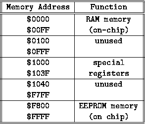
Consider the numeric conversions in Figure 12.1. Notice that four bits equal one hex digit. This is helpful in converting binary to hex. Notice some entries don't have their decimal values filled in. This is to make the point that it is easy to transcribe between binary and hexadecimal representation, but using decimal is often cumbersome. It is good to know some general quantities. For example, eight bits, or one byte, is 256 values. Then the largest unsigned integer representable in a byte is 255. The largest integer representable in two bytes is 65535. A byte can be used to represent one character of information. A standard has been devised for this, called the American Standard Code for Information Interchange standard, or ASCII code, which is pronounced as "ass-key". ASCII is almost universally accepted for representing the English character set, including upper and lower case letters, numbers, and typical punctuation (like !@#$%&*()). An old competing IBM standard, the EBCDIC code, is largely defunct except on some of their mainframes, but modern computer scientists are presently devising a 16-bit international character code. In the back of the Motorola 68HC11 programmer's handbook is a table of the ASCII codes. The most important thing to know is first that it exists, but then some other details. First, notice that it only uses seven of the eight bits in a byte. So, there are actually only 128 ASCII characters, using the values $00 to $7F hex. Printable characters start at $20 hex (32 decimal). The codes from $0 to $1F are used for things like cursor control, line feeds, and the like. Knowing the ASCII characters becomes important when doing interactive programming on the 68HC11, in which case the user might type ASCII information to the 68HC11 over the serial line, and it would respond in kind. In this case, the programmer must deal with the characters as bytes. Introduction to the 68HC11Memory MapMicroprocessors store their programs and data in memory. Memory is organized as a contiguous string of addresses, or locations. Each memory location contains eight bits of data (this is because the 68HC11 is an 8-bit micro; other processors can have 16 or 32 bits of data at each memory location). The entire amount of memory that a processor can access is called its address space. The 68HC11 has an address space of 65,536 memory locations, corresponding exactly to 16 bits of address information. This means that a 16-bit numeral can be used to point at, or address, any of the memory bytes in the address space of the 68HC11. Thus four hexadecimal digits (4 bits per digit 4 digits) can exactly specify one memory location (in which the user will find one byte of information). In general, any area of memory should be equivalent to any other. Because the 68HC11 is a special-purpose chip, and all of its memory is etched right on the microprocessor chip itself, its designers had to dedicate portions of its memory to particular functions. Figure 12.2 shows a "memory map" of one of the members of the 68HC11 family of processors, the MC68HC811E2FN.
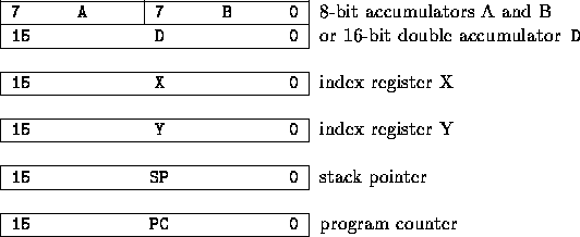
The first area of memory, from address $00 to $FF, is the chip's random access memory, or RAM. RAM can be both written and erased. It is "volatile," which means that when power is removed from the chip, it loses its state. RAM is typically used for storing programs and data. When you program the 68HC11, however, on-chip RAM is not typically used to store programs, because there is only 256 bytes of it ($00 to $FF is 256 bytes). It is normally used to store data and variable values that the program will use while it is running. Programs will reside normally in the external, non-volatile RAM, or in the EEPROM, an acronym for electrically erasable programmable read-only memory. EEPROM is the culmination of a trend in programmable, yet permanent, memory technology. Read-only memory (ROM) means what it suggests: that memory can only be read, not written to like RAM. It is programmed at the factory, in mass quantities. This is good for companies that are selling a production version, but to satisfy R & D engineers, PROM (programmable read-only memory) was developed. PROM chips can't be erased, so in order to make changes to code, the chip is thrown away and a new one is used. PROM chips are not especially expensive, but this process still imposes a high development cost. EPROM, or erasable programmable read only memory, was the next step. Most EPROM chips are erased by exposing the chip to ultraviolet light for half an hour. This is a vast improvement over PROM, but unless there is a large supply of blank chips for reprogramming, the programmer will have a long wait time between code downloads. Many members of the 68HC11 processor family have the latest development in ROM technology: EEPROM, which is electrically erasable. This means that the chip can erase its own ROM, and download new data to be written into it. This allows new programs to be downloaded into the chip in just ten seconds or so. Also, because it is ROM, when the processor is powered down, its program does not go away. EEPROM is not a substitute for RAM: writing new data in is extremely slow by RAM standards, and can only be done a finite number of times (about one to ten thousand erase/write cycles). If present, the EEPROM resides at the top end of the 68HC11's address space. There is 2K of EEPROM (2048 bytes) in the MC68HC811E2FN, from addresses $F800 to $FFFF, and 512 bytes, from addresses $B600 to $B6FF, in most other members of the 68HC11 family. The 'A1 version of the 68HC11 used in ELEC 201 does not have any EEPROM, because the entire external RAM is non-volatile (The part used has internal battery backup). The last hundred bytes or so of the address space, from addresses $FFC0 to $FFFF, are reserved for special interrupt vectors, which are discussed in Section 12.3.8. In the middle part of the address space, starting at address $1000, is an area for special control registers. By storing and reading values from this area of memory, you can control input/output functions like the serial ports, sensors and motor ports, and a host of other 68HC11 special functions. These features are discussed in in Section 12.4. RegistersA microprocessor does its work by moving data from memory into its internal registers, processing on it, and then copying it back into memory. These registers are like variables that the processor uses to do its computations. There are two different types of registers: accumulators, and index registers. Accumulators are used to perform most arithmetic operations, like addition, subtraction, or performing logical and bit operations (and, or, invert). Results of such operations are often placed back into a register; for example, an instruction may add something to the "A" register and place the sum back into that same register. It is for this reason that the name accumulator is appropriate for these register types: they accumulate the results of on-going computations. Index registers are used to point at data that is located in memory. For example, in the add operation just described, the addend (the number getting "added in" to the sum) might be indexed by the "X"' register, meaning that the X register is being used to indicate the address of the data in memory. Figure 12.3 shows the "programmer's model" of the registers of the 68HC11.
The 68HC11 has two accumulators, labeled A and B. Each are 8-bit registers: they hold one byte of data. The general-purpose index registers are the X and Y registers. These are 16-bit registers and are most commonly used to address data in memory. The A and B registers can be used together as a 16-bit arithmetic register, in which case they are named the D register. As indicated in the diagram, the A register forms the "high bits," or most significant digit, in this mode. The Stack Pointer, or SP register, is used to store the location of the program stack. The stack, which is explained in detail later, is used for temporary storage of data, and to store the return address before a subroutine is called. The Program Counter, or PC, is used to keep track of the current instruction being executed. The PC is automatically incremented as the microprocessor proceeds through the instruction stream. Programming the 68HC11When a microprocessor runs a program, it advances sequentially through memory, fetching and executing one instruction at a time. As mentioned earlier, the PC (program counter) register keeps track of the address of the instruction currently being executed. The microprocessor automatically advances the PC to the next instruction after it is finished executing the current one. Consider a typical instruction: load a number into the A register. The machine code for this instruction is (in hex): 86 nn, where nn is the byte to be loaded into the register. The hex value $86 is called the operational code, or op-code, that signifies the "load A register" instruction. Instructions may be one, two, three, or four bytes long, depending on what their function is. When the microprocessor encounters the byte $86 in the instruction stream, it knows, "I'm going to fetch the next byte of data, and load that into my A register." After the microprocessor evaluates the first byte of an instruction, it knows how many more bytes it needs to fetch to complete the instruction, if it is longer than one byte. Then, it executes the next instruction, and so on, ad infinitum. Instructions take varying numbers of machine cycles to execute, depending on their complexity. The 68HC11 for ELEC 201 operates at a frequency of 2 megahertz (MHz.), meaning that it executes 2,000,000 machine cycles per second. The period of a machine cycle is then 0.5 microseconds (sec), so an instruction that requires 3 machine cycles will take 1.5 sec of real time to execute. In general, longer instructions (those needing two, three, or four bytes) take longer (more machine cycles) to execute, although there are some exceptions to this rule. Machine Code vs. Assembly LanguageThe terms machine code and assembly language refer to the same thing: the program that is executed directly by the microprocessor. However, these terms refer to the program in different states of development. Machine code usually refers to the raw data stored as a microprocessor's program. This is commonly described in the hexadecimal notation we've been using. Assembly language is a set of mnemonics, or names, and a notation that is a readable yet efficient way of writing down the machine instructions. Usually, a program that is written in assembly language is processed by an assembler program, that converts the mnemonic instructions into machine code. This output from the assembler program is often called the object code, which can then be executed directly by the microprocessor. In the 68HC11 assembly language, the "Load A register" instruction that we discussed earlier is written as follows:
LDAA #$80
The word "LDAA" is the assembly language mnemonic for "LoaD Accumulator A." Then, the #$80 is the hexadecimal value to be loaded (the value $80 was chosen at random). When a 68HC11 assembler program processes an input file, it knows the mnemonics for all of the 68HC11 instructions, plus their corresponding op-codes. It uses this information to create the object code file. The assembly process is a straight-forward, mechanical operation. Each assembly-language instruction is converted to one machine-language instruction (though that instruction may be one to four bytes in length). Assembler programs lack much of the sophistication that high-level language compilers must have. But, assemblers typically have features to make writing assembly programs easier. These features allow the creation of symbolic labels for constant values or memory addresses, perform arithmetic in binary, decimal, and hex format, and convert character strings to binary values (among other functions). The basic Motorola 68HC11 assembler is described in Section 12.5. The assembler cannot be used to directly build ".icb" files suitable for downloading. Rather than presenting an overview of assembly language all at once, 68HC11 instructions are introduced throughout this document in a progressive fashion. Addressing ModesIn our previous example (LDAA #$80), the hex value $80 is loaded into the A register. This method of loading data into the register is called immediate addressing, because the data to be loaded is located "immediately" in the instruction itself. Immediate addressing is commonly used to load a known piece of data into a register. There are other ways to address data bytes that need to be operated on. These different methods are known as addressing modes. Other than the immediate addressing mode, most addressing modes provide ways of accessing data that is stored somewhere in memory. The extended addressing mode is one way to access data stored in memory. In this mode, the 16-bit address of a memory byte is specified in the instruction. For example, the instruction LDAA $1004 will load the A register with the contents of memory location $1004. This instruction uses three bytes of memory: one byte is the op-code, and two more bytes are needed to specify the 16-bit memory address. The direct addressing mode is similar to the extended mode, but works only for data stored in the first 256 bytes of the chip's address space, from addresses $00 to $FF. This happens to be the chip's RAM, as shown in Figure 12.2, the 68HC11 Memory Map. So, the direct mode is used to store and load data to the RAM. In the direct mode, only one byte of address data is required to specify the memory address, since it is known to be in the first 256 bytes of memory. Instructions using direct addressing may require only two bytes: one for the op-code, and one for the address information. They execute in fewer cycles as a result of this savings. The 68HC11 assembler will automatically choose the direct addressing mode if the address specified is in the range $00 to $FF. Extended addressing could also be used to access this portion of memory, but it would rarely be preferable. The indexed addressing mode uses the X or Y register as a pointer into memory. The value contained in the index register and an offset byte are added to specify the location of the desired memory byte or word. Consider the following example: Suppose the X register currently has the value $1000. Then the instruction LDAA 0,X
will load the A register with the contents of location $1000, and the instruction LDAA 5,X
will load the A register with the contents of location $1005. The offset value is contained in one byte of data, and only positive or zero offsets are allowed. This means that only offsets in the range of 0 to 255 decimal are possible. Why would a programmer use the indexed addressing mode, when the extended addressing mode will access the desired byte directly? The indexed addressing mode is useful when you are repeatedly accessing locations from a particular region of memory, and is useful in part because of the associated offset bytes. For example, the 68HC11 special register area begins at location $1000 and ends at location $103F. Suppose there were a series of instructions that accessed the registers located in this area. We could then set up the X register as a base pointer, pointing to the beginning of this area of memory (we'd load the X register with $1000: LDX #$1000). Then, we can use the two-byte indexed instructions to do a series of loads, stores, etc. to the locations in this region in which we are interested. This is good programming practice because each indexed instruction saves a byte over the extended instruction. Once the cost is paid of loading the X register with the base address (a three byte instruction), each use of an indexed instruction will save code space and execution time. Indexed addressing is most useful when working with arrays of common data structures. Then, one can set up an index register to point at the base of each data structure and use indexed operations to access individual fields of that data element. To move to the next data element, only the index base pointer needs to be changed, the offsets will then access the subsequent structure. Finally, there are a few instructions that do not support the extended addressing mode (they support only direct and indexed addressing), so if one must work with a byte not in the direct addressing area, then indexed addressing must be used. Here is a list of all of the addressing modes that are supported on the 68HC11 architecture:
Data TypesThe 68HC11 supports a few different "data types," or ways of representing numbers. Most high-level languages (like C) support many data types, such as integers, floating point numbers, strings, and arrays. In assembly language, a programmer is given only "the bits" and must build more complex data types with subroutine libraries. The 68HC11 has two data types: 8-bit numbers and 16-bit numbers. This means that there are instructions that process numbers of length eight bits (bytes), and there are instructions that process numbers of length sixteen bits (words). Keep in mind the range of an eight-bit number versus a sixteen-bit number. An eight-bit number can have 256 different values (), and a sixteen-bit number can have 65536 different values ( ). Arithmetic OperationsMicroprocessors give the programmer a standard set of arithmetic and logical operations that can be performed upon numeric data. The 68HC11 provides instructions that work on both eight-bit data values (such as the A or B registers or memory bytes) and sixteen-bit data values (such as the X and Y index registers). Earlier processors provided only eight-bit operations; the programmer had to combine them to get sixteen-bit ones. The 68HC11 also provides multiplication and division instructions. The 68HC11 supports the following instructions:
There are a few arithmetic instructions not mentioned here, but they are relatively obscure. Signed and Unsigned Binary NumbersThere are two methods of representing binary numbers that are commonly used by microprocessors. Using these two methods, the same string of 1's and 0's that comprise a byte or word can represent two different numbers, depending on which method is being used. The two methods are: unsigned binary format and two's-complement signed binary format. The unsigned format is used to represent numbers in the range of 0 to 255 (one byte of data) or 0 to 65535 (one word of data). This is the more simple way of representing data; it is easy to understand because there is a direct translation from the binary digits into the actual numeric value. But, the unsigned format has the limitation that values less than zero cannot be represented. Here are some unsigned binary numbers and their decimal equivalents:
Signed values are represented using the "two's complement" binary format. In this format, a byte can represent a value from to , and a word can represent a number from to . The highest bit (most significant, or left-most bit) of the number is used to represent the sign. A "0" in the high bit indicates a positive or zero value, and a "1" in the high bit indicates a negative value. If the number is positive or zero, then the signed representation is exactly equivalent to the unsigned one. For example, the largest binary number representable in a byte, using the signed format is %01111111. The leading zero is the sign bit, indicating a non-negative number; the seven ones that follow are the significant digits. If the number is negative, then the following process determines its value: invert the significant digits (change zero's to one's and one's to zero's), and add one. Put a minus sign in front of the number, and that is the equivalent value. For example, what is the value of the signed number %10011011? We know this is a negative number, since its high bit is one. To find its value, we take the significant digits ( %0011011) and invert them, obtaining %1100100. We add one, and obtain %1100101. This value converted to decimal is 101; thus, our original number was equal to . Two's complement is employed because it has one very useful property: signed binary numbers can be added together like unsigned ones, and results of standard addition and subtraction processes produce correct signed values. Consider the following example, which shows an addition of two signed binary numbers to produce a valid result:
               10011011     (-101 decimal)
             + 01110000     ( 112 decimal)
             ----------
            (1)00001011     (  11 decimal)
Ignoring the carry out of the highest bit position, we can see that performing regular binary addition on the two numbers gives us the correct result. This is important, because then the microprocessor doesn't have to implement different types of addition and subtraction instructions to support both the signed and unsigned data representations. Condition Code Register and Conditional BranchingWhenever the 68HC11 performs any type of arithmetic or logical operation, various condition codes are generated in addition to the actual result of the operation. These condition codes indicate whether or not the following events happened:
There is a special register in the 68HC11, called the condition code register, or CCR, where this information is kept. Each condition is represented by a one-bit flag in the CCR; if the flag is 1, then the condition is true. The CCR has eight flags in all; four more in addition to the four mentioned. Each flag has a name: the zero flag is called Z; the overflow flag is V, the negative flag is N, and the carry flag is C. The usefulness of these flags is that programs may branch depending on the value of a particular flag or combination of flags. For example, the following fragment of code will repeatedly decrement the A register until it is zero. This code fragment uses the "branch if not equal to zero" instruction (BNE) to loop until the A register equals zero.
Loop    DECA            * decrement A register
        BNE     Loop    * if not zero, jump back to "Loop"
        ...             * program execution continues here
        ...             *    after A is zero
An entire set of these conditional branching instructions allows the programmer to test if the result of an operation was equal to zero, not equal to zero, greater than zero, less than zero, etc. Some of the conditional branching instructions are designed for testing results of two's complement operations, while others expect to test results of unsigned operations. As mentioned earlier, the same arithmetic operations can be used on both signed and unsigned data. This is true, but the way that one must interpret the condition codes of the result is different. Fortunately, the 68HC11 branch instructions will perform this interpretation properly, provided the correct instruction is used for the type of data the programmer has in mind. Here is a list of some of the conditional branching instructions supported by the 68HC11:
Other branching instructions work with signed data and check the proper combination of flags to tell if results are greater or less than zero, etc. One important thing to remember about branching instructions is that they use the relative addressing mode, which means that the destination of a branch is specified by a one-byte offset from the location of the branch instruction. As such, branches may only jump forward or backward a maximum of about 128 bytes from the location of the branch instruction. If it is necessary to branch to a location further away, the JuMP instruction (JMP) should be used, which takes an absolute two-byte address for the destination. The destination of a JMP instruction thus may be anywhere in memory. If necessary, use a conditional branch instruction to jump to a JMP instruction that jumps to far-away locations. Stack Pointer and Subroutine CallsAlmost all microprocessors support a special type of data structure called the stack. A stack stores data in a last-in, first-out (LIFO) method. To visualize the stack, one may imagine a dishwasher who is washing a sink full of dishes. As he washes a dish, he places it on top of a pile of already-washed dishes. When a chef removes dishes from the pile, the dish that she removes is the last dish that the dishwasher placed on the pile. In this way, the stack of dishes stores the dishes using a last-in, first-out algorithm. The stack on the 68HC11 works the same way. Instead of a stack of dishes, the 68HC11 stores bytes in a contiguous area of memory. Instead of a dishwasher and a chef, the 68HC11 uses a special register, called the stack pointer or SP, to keep track of the location of the stack in memory. When a number is placed on the stack (called a stack push), the number is stored in memory at the current address of the stack pointer. Then the stack pointer is advanced to the next position in memory. When a number is taken off the stack (called a stack pull), the stack pointer is regressed to the last location stored, and then the number at that memory location is retrieved. The stack has many different uses. One use is temporary storage of data. Suppose there is a number in the A register to be stored and then retrieved a few instructions later. One could push it on the stack (PSHA) to save it, and later pull it off the stack ( PULA) to restore it. The data in several different registers may be temporarily stored and retrieved in this way. It is important to remember that data goes on and comes off the stack in a particular order. If data is stored with a PSHA and then a PSHB (push A register, push B register), it must restored with the sequence PULB, PULA (pull B register, pull A register). The most important use of the stack is involved with subroutines. Subroutines are pieces of code that may be "called," or executed, by your main program. In this way, they are like utility routines that your software uses. For example, suppose a program often has need to execute a delay, simply waiting of a second. Rather than repeatedly writing the code to perform the delay, it can be written just once, as a subroutine. Then, whenever the main code needs execute the delay, it can just call the subroutine. The key thing about executing a subroutine properly is knowing where to return when it finishes. This is where the stack comes in. When a subroutine is called, the 68HC11 automatically "pushes" the return address -- the place to continue after the subroutine is done -- onto the stack. Then, it branches to begin executing the subroutine. When the subroutine is finished, the 68HC11 pulls the return address directly off the stack and branches to that location. One may think, "Well, we don't need a stack for this; we could just have one particular location where the return address is stored. We could just look there when returning from a subroutine." Actually, that is not a bad solution, but using the stack gives us a special power: it enables nested subroutine calls. What happens when a subroutine calls a subroutine? If a stack is being used, the second return address simply gets pushed on top of the first, so that the first return address remains intact. In the other method, the first return address would be overwritten and destroyed when the second subroutine call occurred. One detail worth mentioning about the stack's implementation on the 68HC11 is that the stack builds downwards in memory. That is, when a number is pushed on the stack, the stack pointer is actually decremented to point to the next available memory location. This is somewhat counter-intuitive, but it is irrelevant to the function of the stack. Since the stack is a dynamic structure, it must be located somewhere in 68HC11 RAM (read/write memory). It is customary to initialize the stack at the top of user RAM. Then, as the stack grows, it moves downwards towards location $0000. A good way to crash the processor is to repeatedly push a value on to the stack and forget to pull it off. If this mistake is made inside a program loop, all of RAM will easily be filled with garbage. When a subroutine attempts to return to its caller, the return address will be nowhere in sight. Just remember: each stack push must be matched with a stack pull. Each subroutine call must be matched with a return from subroutine. Interrupts and Interrupt RoutinesInterrupt routines are a type of subroutine that gets executed when special events happen. These special events are often called interrupts, and they may be generated by a variety of sources. Examples of things that may generate interrupts are: a byte coming in over the serial line, a programmable timer triggering, or a sensor line changing state. When an interrupt happens, the 68HC11 stops what it is doing, saves its local state (the contents of all registers), and processes the interrupt. Each interrupt has code associated with it; it is this code that is executed when the interrupt occurs. Interrupts may be used to give the appearance that the 68HC11 is doing several things at once. There are a several reasons for this:
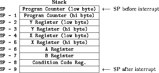
If multiple interrupts are being used, it is possible for an interrupt to occur during the servicing of a different interrupt routine. Typically, interrupting an interrupt routine is not a good idea. The 68HC11 deals with this nested interrupt condition by queueing up the interrupts and processing them sequentially, based on a predetermined interrupt priority scheme. In their usage of the stack, interrupts are implemented quite like subroutines. When an interrupt call is processed, however, the state of all of the 68HC11 registers is saved on the stack, not just the return address. This way, when the interrupt routine returns, the processor can continue executing the main code in exactly the same state that it left it. Figure 12.4 shows the configuration of the stack immediately after an interrupt call.
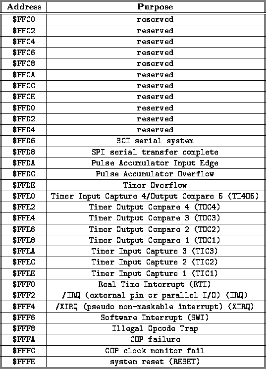
Interrupt VectorsWhen an interrupt occurs, the 68HC11 must know where the code associated with that interrupt is located. An interrupt vector points to the starting address of the code associated with each interrupt. When an interrupt occurs, the 68HC11 first finds its associated interrupt vector, then jumps to the address specified by the vector. These interrupt vectors are "mapped" into specific areas of system memory. In the 68HC11 architecture, the interrupt vectors are located at the top of memory. This area, reserved for the interrupt vectors only, starts at address $FFC0 and continues to the end of memory, address $FFFF. Two bytes are needed for each interrupt vector; thus it may be calculated that the 68HC11 has ($FFFF $FFC0 1) 2 total interrupt vectors. (This is 32 decimal.) The location of each interrupt vector is predetermined. For example, the RESET interrupt is generated when the system reset button is pressed. The RESET vector is located at addresses $FFFE and $FFFF, the very last two bytes of memory. When the reset button is pressed, the 68HC11 jumps to the location specified by the pointer contained in those two bytes. Since pressing reset should restart the microprocessor, the reset vector usually points to the start of the main code. Figure 12.5 shows a map of the memory space from locations $FFC0 to $FFFF and the interrupt vectors associated with each location. Please refer to it later, when we discuss the purpose of some of the vectors that are listed here.
Architecture of the 68HC11The 68HC11 chip includes many features that often must be implemented with hardware external to the microprocessor itself. Some of these features include:
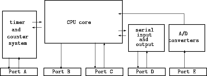
This section explains how to use these advanced features of the 68HC11. Register BlockThe 68HC11 uses a particular area of memory to interface with the special functions. This area of memory is called the register block and is located from addresses $1000 to $103F. The general method of controlling the various features of the chip is by reading and writing data to the different registers in the register block. Since the register block is mapped into memory, the typical 68HC11 instructions for reading and writing data to any area of memory are used to interact with these registers. Block Diagram of 68HC11Figure 12.6 shows a simplified block diagram of the 68HC11 architecture. This diagram depicts the 68HC11 in "single chip" mode, as opposed to the "expanded" mode presented in Chapter 3, and used on the RoboBoard. A more complete block diagram may be found in the Motorola M68HC11 Reference Manual.
When scanning the diagram, notice that some of the ports have arrows running in both directions (ports A, C, and D). These ports are bidirectional, meaning that they can be used for either input or output. Each port contains eight data bits, making it equivalent to one byte of data. Each data bit is mapped to a physical pin on the microprocessor package. This means that when data is written to a particular output port, that data appears as voltage levels on the real pins connected to that port. In this way, the 68HC11 can interface with external devices. In many cases, ports may contain a mixture of pins used for either input or output. In other cases, particular pins in a port are dedicated to a specific function. Following is a brief description of each port on the diagram. The rest of this section explains how to use each port in detail.
The following section begins the in-depth explanation of these ports with Port B. Port BPort B is controlled by a register located at address $1004. In the 68HC11 literature, this register is named PORTB. Port B is implemented as eight output pins on the 68HC11. The following two instructions write the value %00010000 at the Port B register location, $1004.
        LDAA    #%00010000
        STAA    $1004         * store A at "PORTB" location
Port CPort C may be configured as an output port and used in a similar fashion to Port B using the DDRC (data direction for Port C) register, as detailed in the Motorola literature. Port C is controlled by reading the value of the location $1003. Whatever input signals that are present on the Port C lines are "latched" into Port C during the read operation. The Port C register is referred to by the name PORTC. The following code sample reads the digital inputs from Port C and branches to the routine called AllZero if the input from Port C is zero.
        LDAA    $1003    * load Port C value into A
        BEQ     AllZero  * if zero, branch
Analog Input PortPort E is the analog input port. This port is controlled by several registers and may be configured in a few different ways. In order to use the analog-to-digital (A/D) converter, the A/D system must first be powered-up (its default state is off). The System Configuration Options register (OPTION) is used to turn on the A/D system. Bit 7 of this register must be set to "1" in order to turn on the A/D system:
        LDAA    #%10000000    * bit 7 set to 1
        STAA    $1039         * location of OPTION register
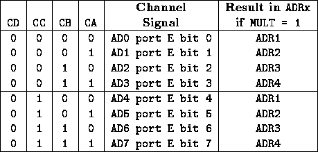
The A/D system is actually configured as two banks of four channels each. In one of its operating modes, it repeatedly samples values from either of these four-channel banks. In another operating mode, the A/D system will repeatedly sample only one of the eight input channels. Because sampling takes a finite amount of time (about 17 µsec), this is a useful mode if one wants to look at one channel very closely. The A/D Control Status Register (ADCTL) is used to select these different modes. Figure 12.7 is a pictorial of the ADCTL register. Bit 7 of the ADCTL register, CCF, is the Conversions Complete Flag. It is set to "1" when the A/D system has finished converting a set of four values. It is important to wait for this flag to be set only when the mode is changed of the A/D system. Then, the CCF will be set to zero, and one should explicitly wait for it to turn to one before trusting the converted values. Bit 5 is SCAN, the Continuous Scan Control. If this bit is set to one, the A/D system will repeatedly convert values. If it is set to zero, the A/D will convert four values and stop. For typical usage, it is probably simpler to set it to one and expect the A/D system to continuously convert values. Bit 4 is MULT, the Multiple Channel/Single Channel Control. If this bit is set to one, the A/D will convert banks of four channels. If it is set to zero, the A/D will convert one channel only. Bits 3 to 0 select the channel(s) to be converted. The results of the A/D conversion appear in four other registers called ADR1, ADR2, ADR3, and ADR4. Figure 12.8 is a table that maps the settings of the channel select bits to the readings that appear in the ADRx registers when MULT equals one. If MULT is zero, then the channel select bits select the channel that gets converted into all four ADRx registers.
Timers and CountersPort A implements a complex set of timer and counter hardware. This section will introduce some of the hardware features; for a more complete description of the timer/counter system, refer to the pink book, The Motorola M68HC11 Reference Manual. TimersThere are five output timers. Each timer has independent configuration settings. Each timer may be programmed to take an action on its output pin when a period of time elapses. Four possible actions may be taken: do nothing, set the output high, set the output low, toggle (invert) the output value. Each timer may be programmed to generate an interrupt when its time period elapses. Typically, the interrupt is used to set up the timer again for its next cycle. Each timer measures elapsed time by using a single 16-bit free running counter, or TCNT. Every timer has its own 16-bit output compare register that it compares against TCNT. When the value of TCNT matches the value in a timer's output compare register, then the timer takes its programmed action (changing its output state, and/or generating an interrupt). A typical way to generate a square wave on a timer output is to write a delay value into the timer's output compare register. The period of the square wave is determined by the length of time that TCNT must count in order to match the timer's output compare register. By writing new values into the output compare register, the timer can be set up to wait until TCNT advances to match it. The following code uses timer 4 to generate a square wave. The square wave is interrupt-driven: each time that TCNT advances to match timer 4's output compare register, the interrupt routine writes a new value into the output compare register, setting up the timer for another half-wave cycle. The SetUp portion of the code enables timer 4's interrupt, and sets up the timer for a toggle each time the compare matches. Assume that the interrupt vector for the timer points to the routine Tim4Int. This routine reads the value in the timer's output compare register, and adds the value 1000 decimal to it. This way, TCNT will have to run for another 1000 counts before the timer toggles its output again. The default speed for TCNT is 500 nanoseconds per count, so the half-wave period of the resulting square wave will be 500 ns 1000, which is 0.5 milliseconds. The full square wave would have a period of 1 msec, or a frequency of 1000 Hz.
SetUp   LDAA    #%00000100    * timer 4 for toggle setting
        STAA    $1020         * Timer Control Register 1 (TCTL1)
        LDAA    #%00010000    * timer 4 select bit
        STAA    $1023         * Timer Interrupt Flag enable (TFLG1)
        STAA    $1022         * Timer Interrupt Mask enable (TMSK1)

Loop    BRA     Loop          * do nothing; interrupt takes over
        ...
        ...

Tim4Int LDD     1000          * load D register with 1/2 wave time
        ADDD    $101C         * add to Timer 4 output compare
        STD     $101C         * save sum back for next edge
	LDX	#$1000        * used in next instruction
        BCLR    $23,X $EF     * clears interrupt flag
        RTI                   * ReTurn from Interrupt
CountersPort A also has three "input-capture" registers. These registers may trigger when any of the following events happen: capture disabled, capture on rising edges only, capture on falling edges only, or capture any edge. These registers may be used to time the length of a waveform. Finally, one bit of Port A can be use for a "pulse accumulator" function. An eight-bit register PACNT can be configured to automatically count pulses on this input pin. Real Time InterruptThe 68HC11 also has a real time interrupt (RTI) function. This function generates interrupts at a fixed periodic rate. This function would be useful, for example, in generating a pulse-width modulated control of the motor output lines. The RTI function can generate interrupts at any of four rates: 4.10 ms, 8.19 ms, 16.38 ms, and 32.77 ms. TMSK2, the Miscellaneous Timer Interrupt Mask, is used to control the RTI system (located at address $1024). Figure 12.9 is a diagram of this register. The RTII bit enables the RTI system when the bit is set to one. Two bits in the PACTL, the Pulse Accumulator Control Register, are used to control the rate of the RTI interrupts. The following table shows the relationship of the RTR1 and RTR0 bits to the interrupt rate.
The PACTL register is located at address $1026. RTR1 and RTR0 are the one and zero bits, respectively, of this register. See the M68HC11 Reference Manual for more details on the RTI system. Serial InterfaceThe serial interface port is controlled by five different registers. Of these, the following three are most important:
The following code sample initializes the serial port for transmission and reception of 9600 baud serial data:
        LDX     #$1000            * used as index register
        BCLR    SPCR,X #PORTD_WOM * turn off wired-or mode
        LDAA    #BAUD9600         * mask for 9600 baud speed
        STAA    BAUD,X            * stored into BAUD register
        LDAA    #TRENA            * mask for Transmit,Rec. enable
        STAA    SCCR2,X           * store in control register
The following code transmits a character and waits for it to finish tranmission:
        LDY     #$1000              * used as index reg
        STAA    SCDR,Y              * store A reg in SCDR
WCLoop  BRCLR   SCSR,Y TDRE WCLoop  * wait until data sent
The following code receives a character from the serial port:
        LDX     #$1000              * used as index reg.
RCLoop  BRCLR   SCSR,X RDRF RCLoop  * wait until char ready
        LDAA    SCDR,X              * input character to A
See the M68HC11 Reference Manual for more details on the SCI serial system. The Motorola 68HC11 Assembler (AS11)LabelsThe assembler has a facility to generate symbolic labels during assembly. This lets one refer to the location of an instruction using a label rather than by knowing its exact address. The assembler does this by using a two-step assembly process. In the first step, the lengths of all instructions is determined so that the labels may be assigned. In the second step, instructions that used other labels have their values filled in, since those labels are now known. Here is an example of a program that uses a symbolic label:
Loop    LDAA    #$FF    * load A with 255
        DECA            * decrement A register
        BNE     Loop    * branch to Loop if not zero
Labels must begin in the first character position of a new line and may optionally end in a colon (:). Arithmetic ExpressionsThe assembler supports the following arithmetic operations, which may be used to form values of labels or instruction arguments:
Expressions are evaluated left to right and there is no provision for parenthesized expressions. Constants are constructed with the following syntax:
Assembler Pseudo-OperationsAn assembler program typically has its own set of commands, called pseudo-operations or pseudo-ops, used to direct the assembly process. These pseudo-ops seem like real 68HC11 instructions, but they are interpreted as control information to the assembler rather than assembled into machine code. ORGThe ORG pseudo-op, for ORiGin, specifies the location for the assembler to deposit the machine code (or object code). In 68HC11 programming, all code should be preceded by the following ORG command:
ORG $F800 * start of \glossary{EEPROM}EEPROM
Observe the following sequence in the RM-11 Monitor program:
        ORG     $F800         * start of EEPROM
Start   LDS     #$FF          * Initialize Stack Pointer
*                               to top of RAM
EQUThe EQU pseudo-op is used to EQUate a symbolic label to a numeric value. Equates are useful so that one does not have to memorize the locations of various 68HC11 control registers; if the registers' names are equated to their locations at the beginning of the code, then one can simply use the labels in programming. The following excerpt illustrates correct usage of the EQU pseudo-op to specify some of the 68HC11 register locations:
PORTA   EQU     $1000   * Port A data register
RESV1   EQU     $1001   * Reserved
PIOC    EQU     $1002   * Parallel I/O Control register
PORTC   EQU     $1003   * Port C latched data register
PORTB   EQU     $1004   * Port B data register
PORTCL  EQU     $1005   * Port C data register
In coding, the programmer may then use the label name rather than the numeric value:
LDAA PORTB * equiv. to LDAA $1004
FCCThe FCC, "Form Constant Character" pseudo-op, deposits a text string into the object code. This is used to store messages in the EEPROM that later can be printed back by the program. The following excerpt illustrates usage of the FCC pseudo-op:
FCC 'Entering repeat mode.'
FCB and FDBThe FCB, "form constant byte," and FDB, "form double byte" pseudo-ops deposit a single byte or word into the object code. They are used to insert data that is not part of a 68HC11 instruction. Example:
        FDB     $1013
        FCB     $FF
RMBThe RMB "reserve memory block" pseudo-op takes an argument and skips that many bytes ahead in the stream of output. It is used to leave a gap in the object code that will later be filled in by the program while it is running.
RMB 10 * reserve 10 bytes
CommentsA comment is:
The * is a special character that can also mean "the address of the current instruction." Thus, the following sequence will create an infinite loop:
BRA * <-- branch to this instruction
Assembler SpecificsThe Motorola assembler is called as11. It is invoked by using the name of the file to be assembled (which typically has the filename suffix .asm):
as11 foo.asm
This will produce a listing of error messages to the screen and the output file foo.s19. The ".s19" suffix indicates the object code file that can be downloaded to the 68HC11. The assembler can be directed to produce an output listing that shows the object code that is created for each instruction. The following invocation will tell the assembler to create a listing file called foo.lis:
as11 foo.asm -l > foo.lis
If writing an assembly language program that will be used with IC, as11_IC is used in place of as11. |
|
|