Elec 422: VLSI Design I
Homework 4
Fall 2003, Tuesday,
October 28, 2003
Independent work is
expected.
Due: Wednesday,
November 5, 2003, at 5 pm.
Problem
1: Pseudo-nMOS Logic
Implement the following circuit in Pseudo-nMOS CMOS
logic as shown. Draw a transistor level diagram of the circuit and use magic_05
and irsim to layout and exhaustively simulate the circuit. Hint: You
will need to modify the length and width ratio between the n-channel and
p-channel devices in the NOR gates for proper operation. Use the: (A) the
standard static complementary CMOS ratio (1 to 2), that is P-channel L=2, W=6,
N-channel L=2, W=3 so L/W ratio is 1 to 2; and (B) a modified ratio as
described in class (4 to 1), both the extra high resistance p-channel pullup
version and the extra low resistance n-channel pulldown version. Please
describe the circuit performance (whether it works logically for all cases)
based on irsim output. Also simulate the circuit with the spice
circuit simulator, for the case where initially (a = 5 V, b = 5 V, c = 5 V, d =
5 V, and then there is a pulse of 19.8 ns. (with rise time 0.1ns and fall time
0.1ns) from 5 to 0 Volts at t = 0 for node a. Nodes b, c, and d will remain at
5 Volts. The total simulation time should be 40 ns. Do this for the standard ratio
1 to 2 circuit and the two versions of the 4 to 1 circuit above.
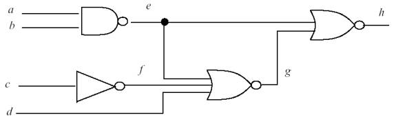
Figure 1: Circuit for
Problem 1.
Problem
2: Domino CMOS Logic
Implement the following circuit in dynamic Domino CMOS
logic (with internal inverters at the output of each gate) as shown. Draw a
transistor level diagram of the circuit and use magic_05 and irsim
to layout and exhaustively simulate the circuit. Hint: You will also need a
precharge signal for this circuit. The gates used below are intentionally AND
and OR structures due to the structural limitations of Domino CMOS in providing
NAND and NOR blocks. Also the test vectors signals a through e
should be low during the precharge phase.
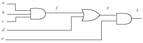
Figure 2: Circuit for
Problem 2.
Problem 3: Basic I/O Pad Behavior.
In order to become familiar with the I/O pads that we
will use this semester for our projects, take the core layout from problem one
and drop it into the 40 pin I/O padframe. Modify your irsim test vectors
used to simulate the design in Problem 1 to now apply the signals from the I/O
padframe by adding the prefix “p_” to the labels on the I/O pads and to your irsim
test vectors. Please make sure that the enable signals for all of the pads are
properly connected to Vdd or GND. Also, please make sure that the enables of
all unused I/O pads are connected to GND to make them input pads. For further
testing, please wire intermediate signals, (e, f, and g) to the output
pads.
The I/O padframe is located at
/usr/site/cad/lib/magic/scmos/pad_06. PadFrame.mag is the main file, and uses
PadVdd.mag, PadGnd.mag, PadFC.mag, and PadBiDir.mag. The file PadBiDir.mag is
the bidirectional I/O pad where the enable signals are connected. There are
additional notes on the class web page concerning the various pad sets.