Elec 422: VLSI Design I
Homework 3
Fall 2003, October 16, 2003
Independent work is expected.
Due: Friday, October 24, 2003, by 4pm.
Timing Analysis: Problems 1 and 2
The following problems 1 and 2 stress the area of timing analysis, based on the papers by Karplus. I have coarsely sketched the main units in the system. You may need to add Latches, and AND/NAND gates in several places for the system to conform to the timing discipline. The Latches prevent problems due to feedback through the circuit, and the AND/NAND gates are needed to qualify the latch control signals.
This assignment is intended to help with some of the high-level timing issues in your design project. In this assignment, you may ignore the actual functionality of the designs.
1. You should add timing labels on each of the “wires” interconnecting the circuit blocks with Valid, Stable, and Qualified clock signals.
2. Create a meg description of the PLA needed to control the adder circuit. Produce a magic_05 file (0.5 micron design rules) for the PLA and simulate the PLA with irsim. Simulate the following computations:
M1 = A1 + B1 + C1 + D1
M2 = A2 + B2 + C2 + D2
M3 = A3 + B3 + C3 + D3
on both hardware systems. You will need to run the systems through enough states to complete the computation.
3. Show on the block timing diagram sktech which cycle the signals will operate on by using the cycle subscript notation introduced in class, (for example Vb2Sa3).
4. You do not need to produce magic layout for the latches, adder, and transmission gates; that is, only magic layout for the PLA.
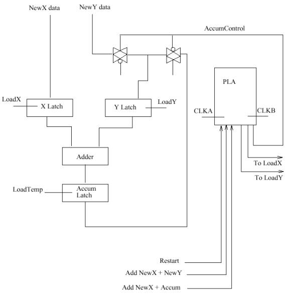
1 Accumulator Based System
This system uses a single adder and an accumulator register. The adder is busy on every clock cycle. It will take several cycles to complete the computation. You cannot start work on M2 until M1 is finished, similarly M3 waits until M2 finishes, so this will be sequential operation.
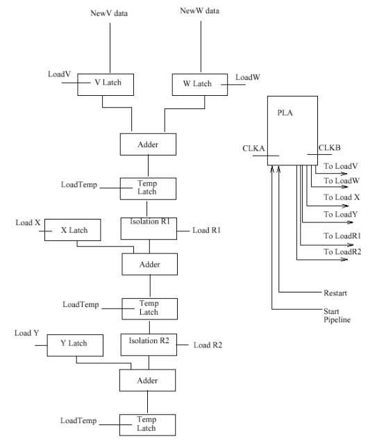
2 Multiple Cycle System (Pipelined)
This system uses several separate adders to complete the computation. Each adder will only be used once to compute M1. You can begin the calculation of M2 = A2 + B2 + C2 + D2 while the calculation of M1 is still ongoing, since registers separate and isolate the computations. Please describe the timing so that the pipeline fills properly and then flushes properly when computation is done. That is, the pipeline should be active only to complete the set of computations desired. Please show how this would work for three sets of results, M1, M2, and M3. The pipeline filling and especially the flushing steps are important in this problem.
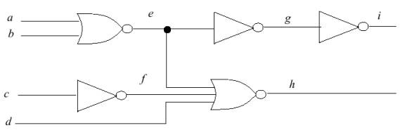
3 Timing Analysis with Crystal
Design the following circuit using magic_05. You may use cells that you have designed for previous homeworks. Use crystal to determine the longest path for the following unclocked circuit. Hint: Read the crystal manual page and the tutorial at the end of the VLSI manual, posted on the class web page.
1. From the crystal results, list the longest and second longest path through the circuit (See note below).
2. On a cif2ps or pplot plot of the complete circuit, trace (in color, by hand) the longest path through the circuit that crystal discovers. Trace the second longest path on an additional copy of the cif2ps or pplot plot. This may or may not be related to or a subset of the first, longest path. You may need to add extra labels to your circuit to make sense of the intermediate nodes that crystal traces through.
Note: You will need to prepare “delay” statements for these experiments. There will be 32 possible cases of “delay” statements based on the four inputs and all transitions to high and low. Some of these will turn out to be equivalent, because of the logic configuration. There are only two outputs to watch “h” and “i”. What we are looking for is the longest paths (either rising or falling) based on the delay patterns of signals rising and falling at time equal to zero at the input nodes a,b,c, and d. Sixteen delay experiments will be sufficient for this assignment, (a rising at t = 0 with b, c, d always 0, a rising at t = 0 with b, c, d always 1, a falling at t = 0 with b, c, d, always 0, a falling at t = 0 with b, c, d always 1. Similar patterns for b rising holding others at 0 and 1, and so on.) Obviously, many of the cases will yield identical results in this simple circuit, but we are trying to
focus on the simulation methodology.
Also Note: The crystal model files that we have are for an older process. Please look at the class notes on the crystal example files, and on the options for the graphics overlay
using “options graphics magic units 0.3” in the crystal vector file.