Elec 422: VLSI Design I
Homework 2
Fall 2003, September 30, 2003
Independent work is expected.
Due: 4pm Friday, October 10, 2003.
For each of the following
problems:
(a) draw a state transition
diagram. Label each state and also label each edge with the appropriate inputs
and outputs.
(b) create a meg description
of the state machine.
(c) create the PLA. Use the
shell script platool_subm which runs meg, eqntott, espresso,
and mpla for the AMI 0.5 micron process.
(d) Using magic_05,
edit the resulting PLA and connect the input state bits to the output state
bits. Use metal and not poly to do the wiring. Also, connect the two
sections of Vdd with a metal line, and fix any possible substrate contact
problems in the upper left corner.
(e) Extract the circuit and
create a sim file using ext2sim -R -t !,
(f) perform a thorough irsim
simulation. Begin by asserting the RESTART signal and then provide
inputs to show that the PLA sequences through the proper states by watching the
state bits, and
(g) draw a logic/block
diagram of the PLA and other circuits as described in the problem. Label the
inputs and outputs of the PLA and the other circuit blocks with the appropriate
labels for system timing, eg. V1, V1S2, etc, as discussed in the paper
by Karplus. (This is very basic in the first problem PLA, but requires some
analysis for the second problem.)
Notes:
The shell script platool_subm
has been updated to use the current PLA template for Revision 6 MOSIS rules
and is compatible with the spacings for the 0.5 micron process. The PLA needs
the clka, clkabar, clkb, and clkbbar signals defined in order to
operate. Place inverter cells in the layout to generate the clkabar and clkbbar
signals.
Submit the following
diagrams and printouts with your homework:
(A) State transition
diagram,
(B) Input file to meg,
(C) The meg output
file called meg.summary
(D) A cif2ps or pplot
plot of the PLA and other external circuitry,
(E) The irsim test
vectors and results.
(F) The logic/block diagram
for system timing.
Do
not include the .mag or .sim files.
Again
please send an e-mail to cavallar@rice.edu,
gadhiok@rice.edu, and rpredrag@rice.edu indicating the location
of your magic and irsim files to help with grading. Please do this within 24
hours of handing in your solutions
Problem 1: Automobile Turn Signal Controller
Design a Turn Signal
Controller PLA for a classic automobile, such as the Ford Thunderbird. On the
rear of the car, the Thunderbird had three turn signal lamps on the left and
three on the right.
The lamps flashed in
sequence. The following inputs exist:
RESTART: Resets the PLA to
the idle state where no lamps are illuminated,
BRAKE: All six lamps are on
while this signal is high. If LEFT or RIGHT are also high, then keep one side
of car’s lights steady, but sequence the other side as described under LEFT and
RIGHT below.
RIGHT: After RIGHT goes
high, the following sequence will occur:
step1 step2
step3 step4
000
--> 100 --> 110 --> 111 --> 000 (right-turn tail light sequence)
LEFT:
Similar behavior to RIGHT.
The following outputs exist:
L0, L1, L2: The left turn
signal lamps.
R0, R1, R2: The right turn
signal lamps.
ERROR: Asserted when both
inputs RIGHT and LEFT are high simultaneously. The other lamps (L0, etc.)
remain low.
Test the following sequence
of operations with duration in clock cycles in parentheses:
RESTART(1), idle(1),
LEFT(8), LEFT and
BRAKE (4),
idle(1), RIGHT(8),
RIGHT and BRAKE (4), BRAKE (3), LEFT and RIGHT (2), idle(1), LEFT and RIGHT (1).
Problem 2: Code Verifier
This system is made up of a
PLA, four one bit static latches, two exclusive OR’s, a regular AND, and some
other glue logic as coarsely sketched in the figure. Please use the
latch cell from Home-work 1, and the static, complementary XOR cell as
described in class based on the AND-OR-INVERT compound gate structure. Connect
and route the various cells. In the figure below, I have roughly sketched the
high-level interconnection of the components. You will need to take this block
diagram and insert inverters and other “glue” logic as needed. I have
intentionally left control signals unconnected, so that you can refine and
finalize the design.
The test vectors should only
contain the inputs and system inputs listed below. The PLA should be creating
the latch control signals, and outputs. The PLA outputs should be qualified
with the system clocks to produce appropriate control signals for the latches.
The inputs are: RESTART
LOADPATTERN LOADTEST ENTER A B CD.
The system inputs are: Vdd,
GND, clka, clkb.
The outputs are: MATCH
ERROR.
Important internal signal:
SAME.
RESTART, LOADPATTERN,
LOADTEST, ENTER are inputs to the PLA. A B C D are inputs to the various
latches.
The PLA behaves as follows:
Upon RESTART, the PLA goes
to an idle state. When LOAD-PATTERN is asserted, the PLA asserts the
appropriate control signal to cause the PATTERN latch to load new data from
inputs A and B. After the data has become valid, the ENTER signal is asserted
to the PLA for one clock cycle and data is stored in the PATTERN latch
and the PLA goes to a wait state. (This protocol is intended to mimic some type
of switch debouncing.)
When LOADTEST is asserted,
the PLA asserts the appropriate internal control signal to cause the TEST latch
to load new data from the inputs C and D. After the data has become valid, the
ENTER signal is asserted to the PLA for one clock cycle by the user and
data is stored in the TEST latch.
The XOR’S then compare the
contents of the PATTERN and TEST latches and AND the results of the individual
bits to produce a SAME signal which is input to the PLA. After the above
loading of the TEST data, the PLA will expect the SAME signal to be calculated
on the following cycle and will assert the MATCH signal if the PATTERN and TEST
are the same. Else it will assert the ERROR signal.
The PLA will continue to
assert either the MATCH or ERROR signal even after returning to a wait state.
The new value of MATCH or ERROR will be calculated after the completion of a
new LOADTEST, SAME sequence.
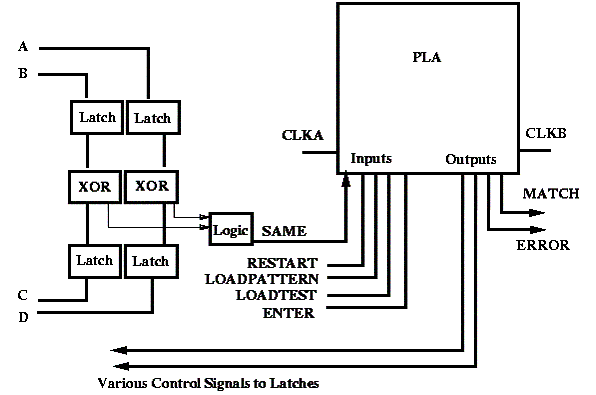
Figure 1: Diagram of the
Code Verifier for Problem 2.
Note 1: Please route Vdd and GND to
your custom logic blocks and also to the PLA so that all power and ground nets
are connected, (no isolated unconnected portions.)
Note 2: Please copy output CIF file
to sub-directory and read back into magic to identify and correct errors around
nwells and substrate contacts.
Note 3: Please qualify the control
signals to the latches with the appropriate system clock signals (clka, clkb)
as appropriate to satisfy the timing requirements.