ELEC 422 / 527, VLSI Systems Design
Course Description, Spring 2024
Instructor:
Joseph Cavallaro, Duncan Hall (DCH) 3042, x4719, cavallar@rice.edu
Office hours: T, Th 2:30 to 3:30 pm after class
Course Schedule:
Credits: 3
Class Contact hours: Day and Time: T, Th 1:00 - 2:15 pm, Location: Ryon B10 lab.
Additional meetings to discuss group project progress will be arranged.
Grading:
Six Homework assignments during the semester. (60%) (Independent work under the Honor System).
Group Design Project (Groups of 2 or 3 depending on class size) (40% total).
a. Group Project Presentation, Design Reviews and Class Participation (10%).
b. Group Project Report (Due last day of finals, April 30, 2024) (20%)
c. Group Project Mask Design (CIF/GDSII) File simulated and integrated into pad frame (Due last day of finals, April 30, 2024) (10%).
Class participation:
Students are expected to attend both class lecture and project group meetings and are encouraged to ask questions throughout the semester.
Course Textbook (Required):
Weste and Harris "CMOS VLSI Design: A Circuits and Systems Perspective" Third Edition, Addison-Wesley, 2005. ISBN: 0-321-14901-7
We plan to use the Third Edition this year instead of the Fourth Edition. Both are similar and are available on-line as used. The Fourth Edition is available at:
https://www.amazon.com/CMOS-VLSI-Design-Perspective-Hardcover/dp/B011DAYZTC
Course Description:
A study of VLSI technology and design. MOS devices, characteristics, and fabrication. Logic design and implementation. VLSI design methodology, circuit simulation and verification.
Prerequisites:
ELEC 326 or a course on digital logic design.
Course Status:
A selected Specialization Elective for majors in Electrical and Computer Engineering
Course Websites:
We will be using Canvas for the assignments and lab projects and announcements. Also, class notes and readings will be posted to the Canvas site. This syllabus will also be posted to the external Web Page: https://www.clear.rice.edu/elec422/
Course Goals and Objectives:
At the end of the course, students should be able to understand and analyze the hardware components of a modern application specific integrated circuit (ASIC) and very large-scale integration (VLSI) technology. They should be able to apply this knowledge to create hardware elements to enable new applications. Also, they should be able to evaluate the efficiency and effectiveness of their solutions and remember the basic structure of hardware components and the basic syntax of hardware description languages and computer aided design (CAD) tools.
Course Outcomes: Related to ABET Criterion 3 number 1 through 7:
The relationships to seven criteria are listed with 1, 2, and 3. (with 3 as most related.)
|
1 |
An ability to identify, formulate, and solve complex engineering problems by applying principles of engineering, science, and mathematics. |
3 |
|
2 |
An ability to apply engineering design to produce solutions that meet specified needs with consideration of public health, safety, and welfare, as well as global, cultural, social, environmental, and economic factors. |
3 |
|
3 |
An ability to communicate effectively with a range of audiences. |
1 |
|
4 |
An ability to recognize ethical and professional responsibilities in engineering situations and make informed judgments, which must consider the impact of engineering solutions in global, economic, environmental, and societal contexts. |
1 |
|
5 |
An ability to function effectively on a team whose members together provide leadership, create a collaborative and inclusive environment, establish goals, plan tasks, and meet objectives. |
2 |
|
6 |
An ability to develop and conduct appropriate experimentation, analyze and interpret data, and use engineering judgment to draw conclusions. |
3 |
|
7 |
An ability to acquire and apply new knowledge as needed, using appropriate learning strategies. |
1 |
Course Topics:
The course topics will include:
Logic Design Tools and Simulation:
"Stick" Diagrams, Hierarchical Layout Methodology,
Mask Level Computer-Aided Design Tools: irsim, magic, spice...,
System Level Languages and CAD Tools:
Verilog Hardware Description Language, Siemens/MentorGraphics Modelsim/Questa and Catapult, Synopsys Design Compiler and Hspice/Saber, Cadence Virtuoso and SoC Encounter (EDI)/Innovus, Catapult C, Xilinx Vitis HLS, Xilinx Vivado FPGA (Ryon B10 Lab),
VLSI System Integration:
Datapath Design, State Machine Design and Programmable Logic Arrays,
System Routing, Clock Distribution, and I/O Pads,
Design for Testability, Fault Tolerance, CMOS Processing,
Scalable CMOS Process Design Kits including AMI/OnSemi 0.5 micron, FreePDK 45nm.
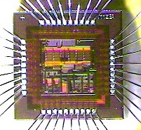
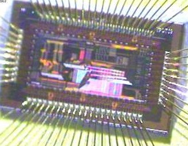
Although we may not have resources to actually fabricate a custom digital ASIC, we will go through most of the steps to tape-out a digital design for a CMOS process.
Laboratory and Design Tools:
We will be using again the CLEAR (Curricular Linux Environment At Rice) Linux cluster in 2024. Several of the design tools have been updated for 2024 and some new CAD tools will be used. Some computer aided design (CAD) tools will be Windows based and most will be on the CLEAR Linux server and require X terminal software such as MobaXterm for Windows or XQuartz for Macintosh. The Ryon Labs B10 lab has 15 Windows computers with MobaXterm installed for access to CLEAR. We will study a broad range of CAD tools for ASIC design and perhaps utilize FPGAs for initial verification and chip testing.
Honor Code Policy:
Project Assignment: When working in groups for projects, your group counts as a single individual for this policy, and your group receives a single score (if equal effort by all group members). You may use your text, course notes, and any other (clearly cited) reference material (that is not a solution). You must clearly list your references in your project report. You may discuss problems, general strategies, or algorithms with other people (in the course or not). When partnering, you should understand and be able to recreate any part of the project solution on your own. For all project assignments, you may NOT use solutions from past classes or found on the web. You may not obtain code from anyone (in the course or not), aside from code provided to you as part of the course.
Homework Honor Code: Complete homework assignments individually. Please list your name on the submitted solution. Solutions submitted after the date and time specified will receive no credit. You may freely use the 2024 course notes, the course textbook, or course handouts for the assignments. Students may discuss and compare ideas on the homework assignments, but each student must write up solutions individually without resorting to copying. That is, students must not create submissions together; students may discuss problems but may not actually write up their assignments together. You should also not refer to solutions posted on the web or from previous years' classes. Clearly state any assumptions that you make to solve the problems and show all your work. You must clearly list any reference material beyond that provided on Canvas that is used.
Generative AI: Large Language Models, such as ChapGPT have emerged recently. The goal of this course is for students to be able to create their own custom C and Verilog code to develop unique ASICs. As such, generative AI methods are not to be used in this course.
Students with Disabilities:
Any student with a disability requiring accommodation in this course is encouraged to contact the instructor after class or during office hours. Additionally, students will need to contact Disability Support Services in the Ley Student Center.
Updates to the Course:
Information contained in this course syllabus, other than the absence policies, may be subject to change with reasonable advance notice as appropriate.
ELEC 527 Additional Course Work:
Graduate students in ELEC 527 will have additional project/report work. This will typically be a research literature survey and analysis report analyzing a current research topic in VLSI Design. The report will be in a 6-page IEEE conference paper format and due at the end of the finals period on April 30, 2024.
Prepared by: Joseph Cavallaro, Date: December 29, 2023